EPROM EMULATOR

As always, all source code and design documents are on my github page: EPROM-EMU-NG on GitHub

I recently posted an article that shows how people ended up using the emulator, check it out there: EPROM emulator NG use cases.

EPROM EMULATOR – An Introduction.

Well, before I explain what an EPROM Emulator is, I should first explain what an EPROM is. EPROM or Erasable Programmable Read-Only Memory is a type of programmable read-only memory that is used to store programs in “computers”. And when I say “computers” I refer to the 80s eight-bit machines (Commodore, Amiga ZX Spectrum, Tandy etc.), but also other computer like devices, controllers etc. that require program memory. Those EPROMS typically come as ICs in DIP28 package with a “window” in the middle used to “erase” the memory using UV light. See below:

Example of EPROM chip used in Commodore 64 “test” cartridge.

So, what is the issue and why would one need an EPROM emulator. By its nature, this type of memory is “read-only” and to change its content you need to erase it with UV light. Imagine you are developing software (well, firmware more likely) and you need to change the “program” in your EPROM memory. That means, remove the EPROM from its host computer, subject it to 20-30min of UV light exposure, program it with EPROM programmer, re-install in host computer. The entire process is extremely slow and has to be repeated every time you want to make even a small one-bit change! And yes, there are modern EPROM alternatives based on Flash technology, that could save you the 20-30 min erase time, but the rest of the process is still the same and still annoyingly slow if you’re writing code and trying to “debug” it.

This is where the EPROM emulator comes in handy, a device that can temporarily “replace” your EPROM chip, it is controlled by a computer and can be reprogrammed in seconds. Once you finish testing you can replace the emulator with an EPROM chip programmed with the final version of your code.

My “EPROM EMULATOR NG” – the “what”.

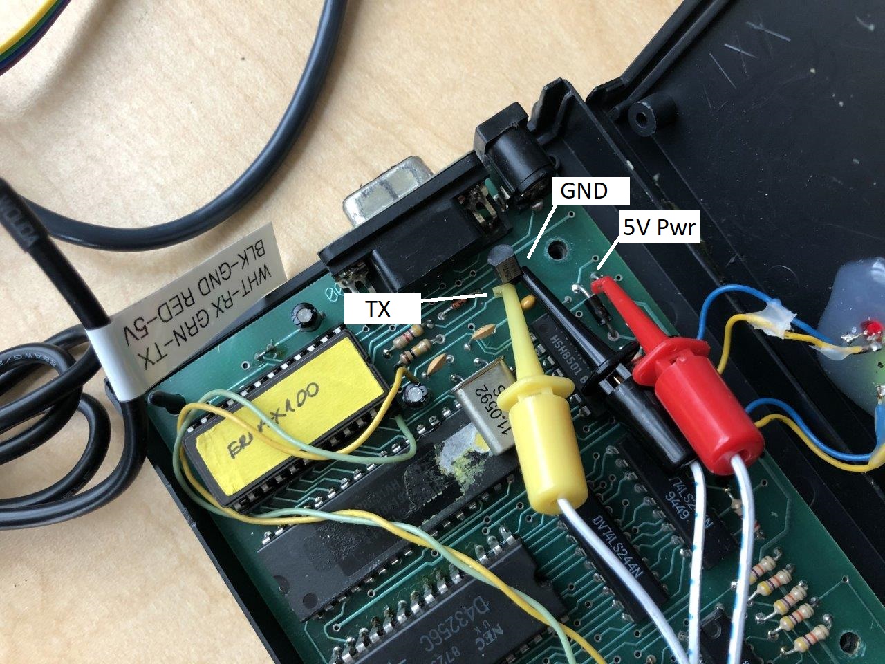
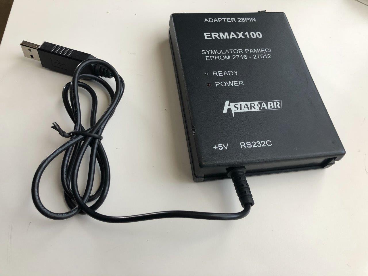
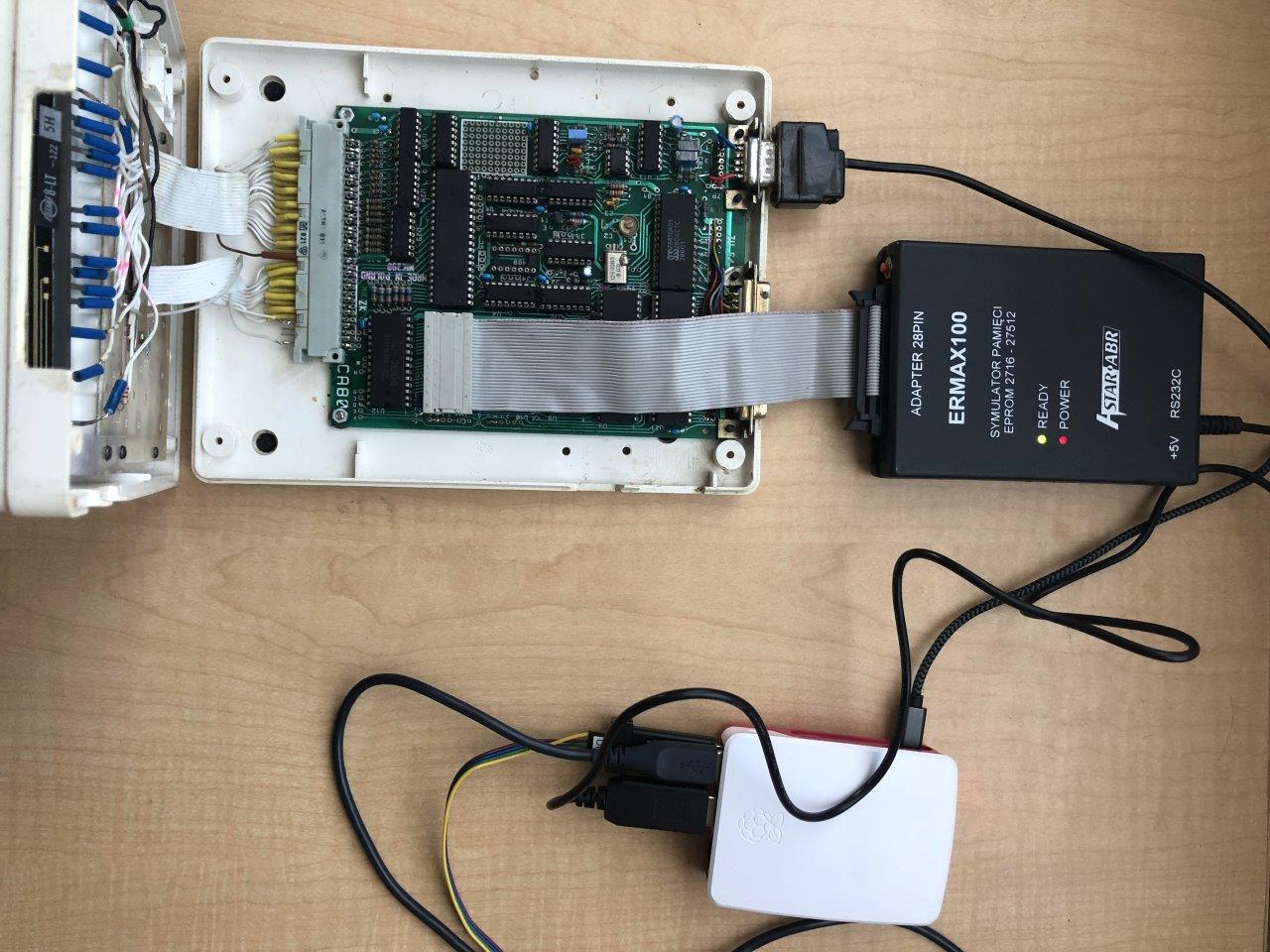
Those who follow my blog know that I already have a commercial EPROM emulator (see the ERMAX100 EPROM Emulator Revival post). I have been using it extensively recently and only just discovered a few really annoying “features” of that emulator. So I was motivated to create something similar to ERMAX 100, but based on a modern microcontroller platform, open-source, cross-platform control software, and free of annoying limitations of my old device (more on that later).

Let’s first have a look at the final result:

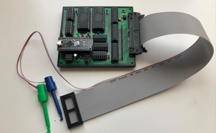
On one end the Emulator has an IDC34 connector J1, where you can plug a DIP28 “probe”, this probe replaces your EPROM device. The probe cable also has two “clips” carrying “reset” signals so you can restart the target platform once new code is uploaded to the emulator. On the “other end” we have a USB (mini in this case) socket allowing connection to the host computer that will control the emulator. The software that controls the emulator is written in Python (3.8) and so far, I have tested it on both Windows and Linux (raspbian) platforms, but should also be compatible with macOS, all basic features are already implemented, but since it’s all open source you can add any other feature you can think of.

The “brain” of the emulator is the Arduino Nano module, the sketch provided in the GitHub repository has most of the features I could think of already implemented. I’m not strong in “C” programming, in fact, the Arduino firmware was based on another project by fellow geek Natasza (check out her memory loader project). It was a good starting point for my implementation, but there is loads of scope for future “improvements”.

Let’s take a look at some examples of how I use the emulator.

My “EPROM EMULATOR NG” – the “how”.

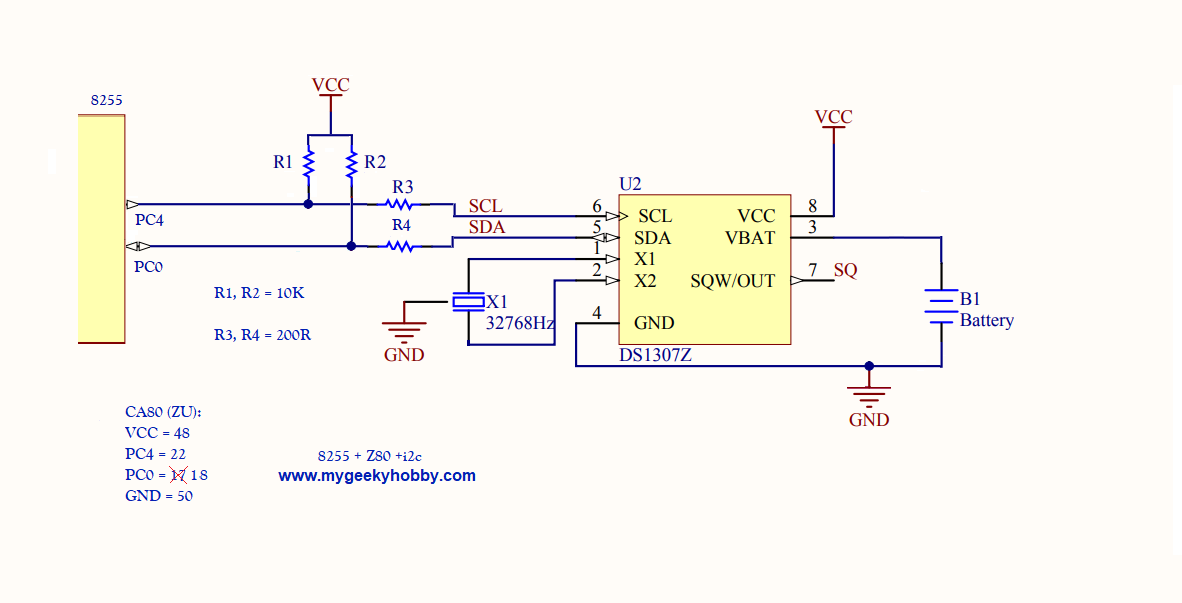
Now we can look into some of the design details, let’s start with the schematic diagram.

There are a few building blocks of the device:

M1 – the Arduino Nano, the “brain” of our emulator – cheap and easy to get. Well-known and supported in Arduino IDE.

U7 and U8 are 32kB static RAM devices (SRAM), together with gate U1B they provide 64kB memory space that will be used to “pretend” or “emulate” the maximum supported 27C512 EPROM. Why am I not using a single SRAM of 64kB capacity you might ask? Those are hard to get today as 64kB SRAM was not very common. In fact, I had quite a few of the 62256 memory ICs spare, plus you can still find this type of memory on Digikey so I decided to stick to those. Why I didn’t use a Flash-based memory instead, well that is a longer story, but I really wanted to just “improve” an existing design of my commercial emulator, and initially didn’t care about the fact the SRAM memory will be cleared when power is gone.

J1 is the connector where we DIP28 “probe” is connected. Details on how to build one of those are also in the GitHub repository.

U9-U11 are 3 state 8-bit buffers, that allow us to “disconnect” the emulator from the target device/machine while we re-program the SRAM.

U4-U6 are serial to parallel “converters” (shift registers) that allow us to generate the Data (8 bit) and Address signals (16 bits) required to control the SRAM, all this using only 6 lines of the microcontroller. Important to note, they have a 3 state output, allowing us to “disable” them from the SRAM bus when the emulator is “running”. Note how the only pin that is unique to each of the shift registers is the data pin, all the other pins are connected in parallel (SRCLK, RCLK, OE etc). This is an unusual configuration, but it allows us to simplify the main routine that shifts the data into the chips, the main loop only needs to do 8 iterations to load all 24 bits (8 of data and 16 of address).

// Write single byte of data to SRAM

void writeMemoryLocation (unsigned short address, unsigned char data ) {
    unsigned char addressHi =  address >> 8 ;
    unsigned char addressLo = address & 0xFF ;    
    unsigned char memData =  data ;
    
    // send data
    
    for (int i = 0; i < 8 ; i++ ) { 
      digitalWrite( DATA, 0x80 & (memData << i) );
      digitalWrite( ADLO, 0x80 & (addressLo << i));
      digitalWrite( ADHI, 0x80 & (addressHi << i) ); 
          
      digitalWrite( SCLK, HIGH );
      digitalWrite( SCLK, LOW );             
    }
    
    digitalWrite( DAT_LD, HIGH ); // latch data and address out
    digitalWrite( DAT_LD, LOW );
    
    // at this point we have data and address loaded into the shift registers
    // now we can request a write to SRAM memory

    digitalWrite( WE, LOW );
    digitalWrite( WE, HIGH );
}

Gates U2A-U2D and U1A allow a to “selectively ignore” address lines A11-A15. Why? Imagine a situation, where you would like to emulate for example a 2764 EPROM, you want to make sure address lines A13, A14 and A15 are ignored in that case, regardless of how they are connected externally to the emulator. This was a major issue for my ERMAX emulator, I was at the “mercy” of how the target EPROM socket was wired in the design. Sometimes even if the device was using a small 27128 EPROM, A15 line would be at VCC (Logic high) so I had to re-map my program to match etc. This new design fixes the issue.

Optional block with the 64kB SPI EEPROM U3 and push-button SW1, was a “design evolution”. Initially, I didn’t care about what happens with the emulator when the power goes “off” – so you lose the “uploaded” image and you have to re-upload when the power comes back “on”. Not an issue when you are writing and debugging your code. But later I realized the EPROM Emulator could be used as a “virtual cartridge” for my Commodore 64, so “restoring” the state of SRAM on power “on” would be useful. I had a choice to totally re-design with Flash-based memory or a simple “hack” by adding the SPI EEPROM and since the SPI EEPROM is also very well supported in Arduino IDE plus I had the required “spare” pins on the microcontroller I decided to go the SPI route. PC control software allows you to decide if you want to upload to SRAM and save to SPI or just upload to SRAM. You also get a choice if you want to “automatically” restore the SRAM from SPI EEPROM on “power on”.

Diode D5 and fuse F1, is a minimal “power management”. The device can be powered by USB-generated 5V from the Arduino Nano or from the DIP28 target device. D5 prevents powering the target from the Arduino, the fuse limits the current drawn from the target if something goes wrong. The diode also protects the emulator from accidentally plugging the DIP28 probe the “wrong way around” into the target. There is some voltage drop on both of those elements. In certain situations, you may want to skip or bypass those. I’m keeping both of them in my emulator and haven’t yet seen issues – but at this point, my design is not widely used so I can’t comment further.

“EPROM EMULATOR NG” – I want one.

So you think it’s a useful device and you would like to own one? You will need to build the hardware first. For that, you should start by getting the PCB. All design files are in my GitHub repository and you can order the PCBs from one of the Chinese prototype houses, I used PCBway and if you don’t have an account yet, you can help me by signing up to PCBWay using my referral link:

PCB from Pcbway

(this will give me a few $ credit for my next project and you will also get a few $ towards your order in return). .

Once you sign up to PCBway, order the project PCB using this link:

PCB from Pcbway

And here is a link to DigiKey cart for PCB hw ver 2.2d, but due to chip shortage quite a few components are out of stock, and here is a cart for hw 1.9d, both include all components required to build the emulator and the probe. The cart total is around $60, you may consider sourcing the Arduino and the flat ribbon cable elsewhere. Other components in the cart are in quantities needed to build a single emulator – but remember you will get 5 PCBs from your order, so might be worth increasing the quantities to build 2 or more :). Also, since you are already paying for the delivery, increase the numbers on some of the common components (one can never have enough decoupling 100nF capacitors).

If you don’t want to build it yourself, I will have some of those devices listed on eBay, including parts “kits” and PCBs:

Once the hardware is built, the rest is just Arduino firmware and python control software, both can be found on my Github page.

As of October 2020, I’ve had reports from many people who successfully built and are now using the emulator. I recorded a quick introduction video that covers the basics of usage. Check out my YouTube channel:

Eprom Emulator DYI – Introduction and getting started on Window(s) 10 🙂

For those planning to build or buy one of my ready devices, I’ve set up a group on groups.io where we can collaborate, feel free to join: https://groups.io/g/eprom-emu-ng

Last note: most of the pictures you see in the above description is v1.0 of the PCB. I built the first 5 prototypes and later discovered an issue with the PCB layout, one of the shift registers (U11) was getting onto a CMOS latch-up state, even though I had a few bypass caps around the PCB, I was still occasionally getting the issues. I fixed my prototypes with a few “bodge” cables.

I improved the PCB design, re-routed some of the power connections and repositioned some of the components, and released as v1.4. At this point the project evolved even further, so what you see on GitHub is PCB v2.1! In the most recent change, I moved from using two smaller SRAM memory chips to using a single larger one. Firmware and software stay the same for both versions.

If you found this helpful and you like the work I do, why not buy me a coffee, thanks! 🙂

Buy Me a Coffee at ko-fi.com

EPROM EMU NG – Use cases.

Here is a couple of examples of how people ended up using my EPROM emulator:

Let’s start with Torsten, who decided to use the emulator to help with the development on his ZX81.

The next one on the list is John and his OMEGA MSX, here is what John shared with me: “Emulator working on my OMEGA MSX (Home built). I use the emulator to emulate cartridge eproms (small games up 64K)”

Leon, the “car hacker” uses the emulator to tune the map inside his car’s ECU.

Richard had a somewhat unusual but very interesting use case:

“Here is a picture of my HP-71b with the HP Curve Fitting 32k ROM loaded in the emulator. Fantastic. I can put my $10 UV Eprom eraser away for good”

Luke is using the emulator to develop firmware for the very popular Ben Eater’s BE6502 “computer”:

“Now I am able to write 6502 assembly in VSCode and use a Makefile to build and deploy the code directly to the BE6502. It even triggers the reset line after code is deployed”

Rick is using the emulator with his Atari 2600

Rene has been working on his 8080 computer and this is what he had to say about the emulator:

“I think, this is a great tool and will make my development much easier. My target: a modular DIY system, developed in Germany in the early 80s. See nkc-wiki.de”

Alexander, my good friend from Canada and his amazing 6802 wire wrapped computer:

Last but not least is Laurent, who is using the emulator to revive some old 8031 projects, Laurent mentions:

your emulator opens a wealth of new possibilities, thank you so much!”

Note how in his emulator the probe connector is soldered on the bottom side of the PCB, turns out there are two versions of the emulator probe DIP28 connector, so he was forced to “mirror” the connections by installing the connector this way.

Hendrik-Jan is using the emulator with a 6502 based KIM-1 clone called PAL-1, he says:

“I’m very thoroughly impressed by everything about this device, both hardware and software...It’s really awesome to see how easy it is to work on some code, assemble it to a binary file and just upload it... just getting to know the emulator, lots to learn, and certainly many different projects to explore in the future (Ben Eater 6502, Commodore 64, RC2014, Microprofessor,  SDK-85, and now soon also MGH80).

Greg built his emulator to develop firmware for a custom Z80 board he is working on, here is what he thinks about the emulator:

“The emulator is an amazing piece of kit that has saved me loads of time especially as a Z80 beginner. I would have had to program an EPROM and swap in and out of the board until my code was working”

Matt is using the emulator on some cool vintage computers, here is what he thinks:

Love the EPROM-EMU-NG, have used it on a Syscom II Apple Clone with mixed up data bit order, and starting work on a Victor 9000″

Rod shared how he is using the emulator in radio hobby, programming his UHF transceiver, he wrote “I have to say it is a great piece of kit“.

A fellow Kris (aka “E-Synthesist”) shared progress of his firmware upgrade project for the Wersi Mk1 synthesizer where he has managed to implement the missing support of the MIDI DUMP function! Apparently, the synth was sold with documentation mentioning this function but it was never actually implemented. Kris developed new firmware that implements the function, here is what he mentioned about the emulator:

“During this project I think I have transferred about 100 interim and test versions of the firmware to the Wersi Mk1. So the project would definitely not have been possible without your EPROM Emulator!”

Mr E.M. from Germany shared his use case, he is working with 8048 CPUs and writing his own assembler. He fully integrated the emulator into his software:

William is using the emulator with the popular TEC-1F computer (Z80):

If you have an interesting use case for the emulator, send me pictures please and I’ll add them here.

Jerome having built the emulator himself, is now using it to write custom programs for the Texas Instruments TM 990/198 single-board trainer/computer. He built a custom emulator probe to support the more unusual TMS2516/2532 EPROMs. Note his “Dollar Tree” lunch box serving a great project box role 🙂

i2c bit-banging on Z80 with 8255A.

This article is mainly aimed at my Polish readers, owners of the educational computer CA80, but the i2c bit-banging for Z80+8255A may come useful on other Z80 platforms. As always source code can be found on my GitHub page.

8255 port control challenge.

There are many websites that cover i2c in detail, so I’m not going to spend any time doing that here, but in the context of this article, the key issue is the fact I’m trying to use a very basic “software-only” implementation of i2c – later used to pull date and time information from hardware real-time clock (HW RTC). I2c uses two lines to implement it’s the bus: SDA (for data) and SCL (for clock). Those two lines have to be independently controlled via software, additionally, SDA is bi-directional, sometimes used as output and sometimes as input. The 8255 offers 3 ports (A, B, C) of 8 lines of general-purpose I/O connectivity. Unfortunately, the way it operates, all lines of each port can only be configured as input or output all at the same time. So if we “plug” our SDA and SCL lines to the same port (for example port B lines 0 and 1), we would not be able to implement the i2c bus this way. The only solution is to use two independent ports (for example port A, and B, or A and C). One more “trick” you can use is the fact that port C, is actually split in half and can be controlled independently (port 0-3 in one group, and 4-7 in another). This is exactly what I’ve done. Let’s see the diagram:

Diagram_v1


As you can see, I’ve used PC.0 for SDA and PC.4 for SCL signals. R1 and R2 are pull-up resistors (I used 10k, but 4.7k would be ok as well) required for all implementation of i2c, R3 and R4 are used for current limiting, for situations where software might be misbehaving sending data at the same time other transmissions are in progress. In my example I’m communicating with a popular RTC from Dallas – DS1308Z (you can use a cheap module from eBay – be aware of issues with those modules where the “trickle charge” circuit may cause the re-chargeable 2032 battery to explode. This has happened to my module, so I removed all the extra components, and I used a non-rechargeable 2032 battery).

The GitHub repository contains the required code RTC_0x2000_0x2300_v1.4.asm The file contains a read and write procedures for the RTC. The code is a bit of a mess of stuff I found on other projects and my own code – but since I haven’t done Z80 assembly language for the last 20 years there is much scope for improvement. Feel free to contribute, but in its current form, the program works and serves its purpose 🙂

The next section is more useful to my Polish audience, so I’ll attempt to write it in Polish.

Dla polskich użytkowników Mikrokomputera CA80 firmy MIK.

Niedawno udało mi się „reanimować” mój emulator pamięci EPROM ERMAX100, wiec w końcu mogę zabrać się ze parę projektów na CA80 które odwlekałem przez prawie …. 20lat.

CA80 to był prawdziwie mój pierwszy…hmm “komputer?”. Poskładałem go jeszcze w podstawówce! I działał. Powstało kilka projektów, pamiętam dobre czasy pisania programów na kartce papieru i „kompilacji” z książką w ręku, oraz żmudne wklepywanie kodu przez klawiaturę CA80.

Dziś, mój CA80 rzadko jest używany (chociaż teraz gdy mam możliwość łatwej emulacji EPROM, mam nadzieję ze to się zmieni). Większość czasu spędza na moim biurku, wyświetlając „CA80”. Dobrze by było chociaż na co dzień używać go jako taki „retro” zegar. Ja mam nową wersje komputera z wyświetlaczem VFD. Niestety brak podtrzymania pamięci czy sprzętowego zegara czasu rzeczywistego (HW RTC) bardzo ogranicza CA80 w funkcji zegara. W tym projekcie chciałem uzyskać następującą funkcjonalność:

  1. Zegar „tyka” gdy brak zasilania – aka HW RTC na magistrali i2c z potrzymaniem bateryjnym.
  2. CA80 automatycznie wyświetla czas gdy zasilanie powróci (komenda *E[0] startuje automatycznie).

Postanowiłem i2c zrobić w programie, poprzez tak zwane „bit banging”. Elektronika to tylko podstawowe elementy standardowej implantacji DS1307Z (gotowy moduł można kupić na eBay za parę dolarów).

Kod źródłowy programu jest na GitHub. Plik RTC_0x2000_0x2300_v1.4.asm należy skompilować darmowym „z80-asm” asemblerem. Jest zaprojektowany by został zaprogramowany do EPROM w podstawce U9 CA80, zaraz ponad podstawowym kodem pod adresem 0x2000h. Ja miałem w U9 pamięć 2764, którą wymieniłem na 27128.

Aby uzyskać automatyczna synchronizację po starcie oraz automatyczne wyświetlenie czasu, należy też zastąpić komendę skoku do głównego menu w monitorze CA80, skokiem do mojego programu:

2764_after

Pod addresem 0x0269h zamienić komendę:

JR START ( 18 05 )

na:

JP 2000h ( C3 00 20)

Na GitHub zamieściłem obraz binarny dla pamięci EPROM 27128 oraz 27256 który zawiera już dodatkowy kod i zmiany w monitorze, należy tylko go zaprogramować i zainstalować w CA80 w podstawce U9 (zakładam ze wszystkie połączenia konfiguracyjne są w fabrycznej pozycji). Elektronikę można zlutować na wewnątrz CA80 lub podłączyć do złącza użytkownika, wymaga tylko 4 połączeń (VCC,GND, SDA-PC.0 i SCL-PC.4).

Program automatycznie odczyta czas i datę po starcie CA80 z HW RTC and nastepnie automatycznie przejedzie do wyświetlania czasu. Wszytkie inne zlecenia powinny działać bez zmian. Do monitora można wrócić naciskając klawisz “M”.

Żeby zaprogramować aktualy czas do nowego układu RTC, należy najpierw ustawić czas w CA80 zleceniem *E[1][sek].[min].[godz]= a następnie wywołać program użytkownika pod adresem 0x2100h komendą *E[G][2100]=, która zapisze aktualny czas do HW RTC.

Kod jest napisany tak “na szybko”, część jest skopiowana z innych projektów online, wyszedłem z wprawy nie pisząc w assembly prze 20lat 🙂 Zapraszam do ulepszenia.

Tymczasem zostawiam was ze zdjęciem mojego CA80, dumnie wyświetlającego czas.

CA_80

ERMAX100 EPROM Emulator Revival

Intro.

I’ve been trying to get back into some of my “retro computer programming”. By the way, “computer” is a bit of an overstatement. As my first “computer” was a very special device, that looked like a calculator and only had an 8 digit 7 segment VFD display – it was called CA80 and was an educational “kit” computer from Poland. I’ll write more about it in the future, for now, I’m just liking to hackaday.io article describing it. One of the challenges of “programming” was that there was no editor on the “computer” and you had to program and compile on paper and once done you had to “punch it in” into the computer by hand. This is not very effective in 2020, so I started looking around for ways to “send” the code directly to the memory of my little computer. And here comes another device from the “days past” – and EPROM Emulator ERMAX100. It was released by a Polish company ASTAR ABR around 1995. By that time I was 15 and in the middle of working on my final year project based on 8051, I was desperate to get my hands on the ERMAX100 so that I can compile the code on my PC (yep at that time I was finally using a proper computer) and send over a serial connection to the emulator that would “pretend” the EPROM memory of my target system. I managed to somehow convince my parents and ended up buying it. I successfully used it for a few years, until devices with builtin flash memory, like the Atmel 89C2051, showed up on the market. Worth noting ERMAX100 can emulate all the common sizes of EPROMs from a 2kB 2716 all the way to a 64kB 27512.

My ERMAX100.

This is my example of the device. At one end the device has just a serial port (RS232) and optional 5V power connector, on the other end the plug for a cable that ends with 28 pin emulator “probe”. There are also two “RESET” hooks, that allows you to reset the target system after the code upload. I’ve added an extra “Reset” button, to be able to reset the emulator itself, as it sometimes “got stuck”.

Ermax100_FB

Here is the emulator “in action”, plugged into my CA80 “microcomputer”.

ERMAX100_CA

The “90s” hardware in the 2020 problem.

Once I got my emulator plugged into the “target” there was a very important issue I was facing. Who still has a serial RS232 compatible port on a computer? I didn’t have one, and I since I wanted the flexibility of being able to plug the emulator to any of my modern machines I came up with a solution: “convert” the device to use USB, to be more precise: replace the RS232 connector on the device with chap USB TTL serial cable.

So I’ve opened the emulator and discovered that it only uses the receive line of the serial port, and the hardware implementation is based on a single transistor. I quickly tested the theory, bypassing the RS232 connector and plugging the TTL-to-USB cable directly to the device:

ERMAX100_TTL_Details

Since that idea worked well, I made it a bit more permanent, first I removed the RS232 connector and the redundant power socket (we can now provide power via USB):

ERMAX100_no_rs232

To re-use the old panel, I filled the holes with epoxy glue and used some black tape to give it a fresh surface. I think the result is acceptable.

ERMAX100_Panel

I’ve attached the 5V, TX and GND lines from the USB-to-TTL cable after removing the transistor that acted as RS232 to TTL converter in the original solution, and secured the cable with a cable tie using two of the holes left after removing the power and RS232 connectors.

ERMAX100_attached

The end result is my ERMAX100 converted into USB 🙂

ERMAX100_USB

The “90s” software in the 2020 problem.

The software that came with it was from the 90s and “it showed”. It was DOS “only” and didn’t run on my Windows 10 machine. Besides that, I do most of my coding those days from a Linux machine (Raspberry pi 4 to be exact).

So I decided to try and “figure out” the protocol and re-implement it in something more platform-agnostic like Python script.

I had to “dig out” one of my older Windows 7 based computers and used it to send a few examples of data using the original software. I then “sniffed” the data on another computer.

ERMAX100_W7

The results were a bit strange:

550301
91ffffffffffffffffffffffff...fff06050403
a2
Total: 4100

550301
90ffffffffffffffffffffffff...fff06050403
a2
Total: 4100

Looks like the format is as follows:

The first byte is a “synchronization” byte of 0x55H, followed by a “type of EPROM” byte of 0x01H for 2716, 0x02H for 2732 etc. The 3rd byte seems to always be 0x01H. Following those 3 bytes is the actual binary file that is the “emulated” data. The last one or two bytes were some kind of CRC check or similar. It was strange as the last  “CRC Byte” was not changing even if I was sending different data (see the example above where my first byte is 0x90H or 0x91H but the CRC stays the same at 0xA2H). Also, the CRC byte and something else was overwitting the last 2-3 bytes of my binary file (again in the example above you can see binary data finishes with 0403, but the original data that I’m sending ends with 04030201). Using different data file I was getting different “CRC” bytes, sometimes even for the same type of file sent multiple times, I was seeing different CRC byte. I the end I assumed that last byte “doesn’t” matter or is not even implemented on the ERMAX100. To test my theory I wrote a simple python script:

import serial,os

ser = serial.Serial('/dev/ttyUSB0',57600, timeout=5)

binary_data = open("C930.rom", 'rb').read()

sync_byte = b'\x55'
mem_type = b'\x04'
is_one = b'\x01' # doesn't matter, code ignores this anyway.

out_data = sync_byte + mem_type + is_one + binary_data

print("Sent: {} Bytes".format(str(len(binary_data))))

ser.write(out_data)
ser.close()

exit()

You will need Python 3.8 and “pyserial” library (“pip install pyserial”). To my surprise, it worked! Even better than the original program, as it wasn’t overwriting the last bytes of my payload with CRC.

Now that I confirmed the “protocol” is correct, I wrote a full script that replaces the original DOS software with a simple Python-based script. I tested it so far on a raspberry pi and a Windows 10 machine both work well. The source is on my GitHub page.

I don’t think there are many people using the ERMAX100 but if you found this article and ended up using the script let me know.

I’m leaving you with some pictures of my ERMAX100 “in action”, emulating the 2764 EPROM of my CA80 microcomputer, programmed from Raspberry Pi 4.

IMG_4343

IMG_4341

Commodore 64 Power Supply 902503-02, part 1.

In my Commodore 64 Power Supply magic post, I talked about the internal power supply and how not everything that you see when you quickly glance is as obvious as it seems. Yet again I’m faced with a similar situation. I needed an external power supply for one of the machines that I purchased recently, and I didn’t want to pay almost the equivalent of half of the cost of the computer for a new power supply. I searched eBay and come across a “faulty, for parts” unit. Perfect for me, as I’ve got a small “lab” at home and I’m able to troubleshoot and hopefully fix it. It was the 902503-02 part number, that as opposed to some of the “newer” version is not “potted” and can be opened and inspected. Before the auction was over I was “researching” the power supply. My “research” started with googling “902503-02 schematic diagram”. The result brings a few similarly looking diagrams, but here is one of the first hits that I found:

902503-02_PSU_baseline

Well, to me it doesn’t look like the original schematic diagram, it’s more of a reverse engineered diagram that someone has created looking at the real circuit of the power supply. We know roughly what to expect on the basis of what I covered in my previous post – two separate outputs: one is unregulated 9V AC, and regulated 5V DC. And at first glance, it sort of looks ok but in reality, this “diagram” is seriously misleading! Here is what I’ve noticed:

902503-02_PSU_errors

Let’s do the “simple” ones first: the diodes have some strange part numbers, in fact, those should be marked 1N5400. The “ground” symbol from the transformer goes nowhere, as there is only one of them. One of the outputs is marked 7.5A … 7.5A!!?? This should be corrected to 7.5VA – alternatively, the entire thing could be just marked 5V/1.5A. But the biggest and a major mistake is the “transistor” marked SK3052P. Yes, it’s a 3 legged device in a “TO-3P package” that looks like a transistor, but it would be impossible to create a 5V regulator based on a single transistor and a resistor. In fact, the “SK” in the part number is a logo for a Japanese company called “Sanken”, the full part number is “SI-3052P” – a 5V at 2A linear voltage regulator integrated circuit. So the author has done the following “mind shortcut”:

3052p

This is very unfortunate “shortcut” as I’ve seen a few posts on C64 forums where people are referring to that regulator as “transistor”! Well now you know it’s not, and the SI-3052P provides a few important functions: it regulates the output voltage at 5V DC independent of the load and it has a built-in overcurrent protection that will “kick in” when the load exceeds around 2.4A. Based on this new information and after “inspecting” one of those power supplies, I’ve re-created the diagram adding a few more details:

902503-02_PSU_my_v1.0

here is full resolution picture

Let me quickly describe what happens: mains voltage is supplied to the primary winding of our power transformer, notice the “protective earth” pin is somehow connected to the transformer (looks like it goes in the layer between the primary and secondary winding) but it doesn’t extend to the output and is not connected to the computer at all. There are two secondary windings:

  • Pin 9 and 11: provides 9V AC that goes directly to the output. Its protected by a 3A fuse F1, I’ve marked the voltage rating of the fuse (250V) but this is not as important on the secondary side, what is important is to know if this fuse is a “slow” or “fast” acting fuse. Unfortunately, the fuse itself doesn’t have any markings saying what type of fuse it is. Inspecting it physically and considering its function I think it’s a “fast” acting fuse. You may ask why do we need this fuse, isn’t there another fuse inside the C64 that is on the 9V AC power rail. It’s true but the fuse here inside the power supply is supposed to protect the transformer form accidental shortcuts on the output before the power supply is even plugged into the computer.
  • Pin 7 and 8: provides 18V AC with a “center” tab on pin 6. This center pin allows the use of two diodes in a full wave rectifier configuration, saving cost by not having to use a 4 diode full bridge rectifier configuration. Next follows a large smoothing filter capacitor C1. This part of the circuit is protected by 5A fuse F2, yet again there is no marking on the fuse, but considering it has to withstand a larger than standard operating conditions initial charging current of the smoothing capacitor and a clearly different physical appearance I deduct it’s the “slow” acting fuse type.

The unregulated voltage from C1 is regulated using U1, the SI-3052P integrated circuit. On the output of U1 we see an additional small electrolytic capacitor C2, that is recommended by the manufacturer to prevent oscillation. There is one more component, the 300 Ohm resistor R1, it’s used to “raise” the output voltage a bit over the nominal 5V to compensate for the losses on the long wires between the power supply and the computer. This is actually very surprising, as looking at the U1 datasheet, we see Note 3: “The output voltage may not be adjusted by raising the ground voltage (using a diode or resistor)”. This is related to the built-in “foldback overcurrent protection circuit” that will be affected if pin 3 of U1 is not at “ground level”. Looks like the engineers designing the power supply ignored the note. When I get a chance I will try to test and compare the behavior of the power supply in a fault condition, with and without that resistor.

Quick comment on the construction of the power supply. The diodes and fuses are soldered directly to the transformer “pins” (with the help of some additional internally unconnected pins 10 and 12). The rest of the components are mounted on a small printed circuit board (PCB). The transformer and the PCB are marked “Billion”, and I assume this is “contract” manufacturer Billion Electric Co., Ltd. of Taiwan, that Commodore tasked with the creation of this power supply.

Lastly, one should note this is a linear power supply, cheap but very inefficient. At full load (C64 plus accessories plugged into the expansion port drawing in total around 1.4), the input voltage on U1 is over 10V, so to “drop” the voltage to 5V on the output the linear regulator has to dissipate close to 8W of power (voltage on input minus voltage on output multiplied by current). U1 and its heatsink get extremely hot, and as we know, hot semiconductors don’t last long…

In part 2, I will cover the restoration/repair of my eBay purchased power supply, I will share some test results and implement few improvements… stay tuned.

Commodore 64 Power Supply magic.

Note:

At the beginning of this post, I cover some basic power supply stuff, so if you already know a lot skip to the later part where I cover the more interesting 12V DC rail.

Not as obvious as it seems.

While browsing “SAMS Commodore 64 Troubleshooting & Repair Guide” I came across the block diagram of the internal power supply system. It was interesting to me for a number of reasons. First, I’m “into” Commodore restorations those days so this generic knowledge is useful, also I hoping to develop a DC only power supply (so that you could run the C64 off of a 12V car power socket). As a reminder this is the block diagram that I’m talking about, from the book:

sams_guide_c64-powersupply_1

Something wasn’t right here… notice the diode on the +9V supply line. My background is electronics, but even though let’s just say I haven’t “practiced” for a while, the direction of that diode makes no sense, it wouldn’t work. Let’s look at the detail diagram from the C64 service manual:

PDU_ServiceManual_Path

Looks familiar? I’ve highlighted the section that I’m wondering about. Seem like the authors of the troubleshooting guide have made a mistake when creating the block diagram, in fact, the diode CR6 (1N4001) has nothing to do with the unregulated +9V power supply line. Since we are already discussing details of the power supply diagram let’s analyze all sections and how each of the power rails is generated one by one:

9V AC

PDU_ServiceManual_9VAC

The 9V AC power is supplied from the external power supply, passes via a common mode choke filter and a fuse. It is then used to generate all other rails plus is made available on the user port pins 10 and 11. Important to note is that the 9V AC rail is also used to generate the 60Hz/50Hz signal for the hardware real time clock built into the CIA chip. This is one of the reasons we can’t replace the external power supply with a modern DC switch mode alternative.

5V DC (+digital)

PDU_ServiceManual_5VDC_digi

Just like the 9V AC, the 5V DC is supplied from the external power supply, it’s filtered and used directly to power majority of the “chips” on-board. Important: since there are no additional components onboard of the c64 handling the 5V DC digital rail, you’re at the mercy of the quality of the external power supply – and we know those old original power supplies are failing a lot. Typically they fail with an over-voltage condition, resulting in “fried” memory and other components, so always check the condition of the external power supply before you use it for the first time.

5V DC CAN (Clock and ANalog ??)

PDU_ServiceManual_5VDC

You may ask yourself why do we need another 5V DC rail, we already have one from the external power supply. Separate, locally generated power is needed for the sensitive video and clock circuits of the computer. The configuration is “textbook” implementation of the 7805 regulator IC. The 9V AC is rectified using bridge rectifier CR4, smoothed using large electrolytic capacitor C19, decoupling capacitor C95 before getting into the regulator. Regulator output is decoupled with C102 and C103.

12V DC

Now we come to the interesting part of my article.

PDU_ServiceManual_12VDC_0

At first glance, you see the 7812 regulator, some bypass components around it (c59, C57, C89, C88) and fed from the 9VAC. But look closely and you see 3 extra components that are not instantly recognized by most: diodes CR6, CR5 and capacitor C90. What are those for? When I first noticed those I came to the conclusion that it must be used to boost the unregulated voltage coming out of the bridge rectifier CR4 and smoothing capacitor C19 to a level required for correct operation of the 7812 regulator – that is typically around 14.6V DC. What I could see from the diagram was:

  • clamper that consists of capacitor C90 and diode CR6, one should note that in our case this is a “biased clamper” type, as the anode of diode CR6 is not connected to ground but to the 9V unregulated dc supply.
  • peak detector (aka half-wave rectifier) that consists of diode CR5, followed by a smoothing capacitor C88.

Ignoring the fact that we are dealing with “biased clamper”, this combination of clamper and rectifier is a typical example of the voltage doubler.

I started “poking” around my Commodore with an oscilloscope (all captures are with 5V / division setting).

9_all

Higher resolution picture here. (btw one day I will learn how to implement a proper gallery in my posts).

Looking at the oscilloscope we see the AC supply entering C90 (bottom right). The amplitude is around 12V, but we can’t fail to notice we only see the positive half of the “AC” signal. This is due to the fact that we are measuring this in reference to the power supply ground, so one of the diodes of CR4 bridge rectifier is forming a half-wave rectifier.

The output from C90 can be seen in the top right and is “shifted” from the ground by the level of “biasing” voltage, in our case, it’s around 10V DC.

Finally, we can see what happens after our supply goes through the half-wave rectifier CR5 and smoothing capacitor C88. Note the output DC voltage that is present on C88 is over 20V. That means that C88 must be rated at 25V minimum. I mention that as I’ve seen people commenting that when “re-capping” capacitors on board of the Commodore you can stick to 16V rated electrolytic capacitors – as you can see this is not true.

All this “complications” mean that it’s not easy to replace the external power supply with a simpler DC switching power supply. Without modifying the internals of your Commodore you will need both DC 5V digital rail and separate 9V AC rail.

Final thoughts.

I hope this was informative. Note that what I described above is what I think is happening, and I’m around 95% sure, but feel free to comment if you think I’m wrong and I will fix it.

I’m working on more Commodore related “material”, so more will follow.

“Pi1541” in 30min with (almost) no soldering.

I need to test my Commodore 64 but I have no floppy drive, cassette deck or cartridge…

This was the dilemma I had one evening after repairing my newly acquired Commodore 64 machine – yes I will write a blog entry about it and link it here later. I really wanted to load a game and test the famous SID chip for it’s sound quality. So off to Google looking for quick solution. There are plenty of those floating around, most are semi-commercial, and pretty complicated and/or expensive, not something you can implement “tonight”. Than I came across the Pi1541 by Steve White. According to his post “Pi1541 is a real-time, cycle exact, Commodore 1541 disk drive emulator that can run on a Raspberry Pi 3B (or 3B+). The software is free and I have endeavored to make the hardware as simple and inexpensive as possible“. Wow, amazing work Steve! Plus he released it all to public for free, including schematic diagram of the “cable” and the source code of his software.

If you follow his post, in his setup instructions you will get to step six where you need to create the cable. There are two versions, simple and more complex. Most of us need the simple version, if fact when you read the instructions you will soon realize the that you can make a “super simple” version of the simple one as there are quite a few “optional” components. So to make the task easy I’ve created a new modified diagram of the “super simple Pi1541 cable”:

mypi1541_v1.0

Full size image here

Yep, that’s it, one component – the 4 channel logic level converter, Steve suggests the Sparkfun part number, but places like eBay, Amazon, Banggood are full of alternatives. All you need is one based on MOS-FET transistors (you will see 4 of the 3 legged tiny transistors on the board) and you’re good to go.

If you want to know what the logic converter does, it’s simple: you can connect to each other 4 digital lines of signals that are not compatible from the logic level point of view – the raspberry pi uses 0V/3.3V voltage to it’s logic “0” and “1” and the Commodore uses 0V/5V voltage. Each pair of HV1/LV1, HV2/LV2, HV3/LV3, HV4/LV4 handles one line, you can imagine that for each pair HV1 pin and the LV1 are “connected” to each other, so if we send a 3.3V “signal” into LV1, it will come out of HV1 as 5V “signal” (note: this conversion works in both directions). The remaining connections are related to power, so you feed “ground” to the GND pins (note: GND pin on the LV side is directly connected to GND on the HV side), you feed the low supply voltage to “LV” pin and the high supply voltage to “HV” pin.

I had one of the Sparkfun parts in my drawer so I decided to go ahead and build the simplified version of the cable, here is what I’ve done:

Step 1.

You need to somehow get the signals out of the Commodore and into the logic converter:

Option A: Get a DIN 6 plug and solder 5 wires onto it, this is what I’ve done:

pi1

“But you promised no soldering”, okay….

Option B: you could “sacrifice” a spare serial cable that you use to connect the original 1541 drive to your Commodore 64, cut it half use one half for your cable and give the there half to one of your friends so they can create a cable for themselves 🙂

Step 2.

You need to somehow connect the cable to the logic level converter, again many options, I soldered a pin header to the logic converter, “crimped” the connectors and used a 6 way plastic plug like this:

pi2

pi3

“But you promised no soldering”, okay….

Option B. You could simply twist the cable into the holes of the logic converter, here is an example of how I would do it if I didn’t know how to solder (example shows different logic converter as I don’t have the 4 channel one handy that doesn’t have pins soldered already):

pi4
First strip a wire about 1cm (0.4inch) and twist it.

pi5
Feed the cable through the hole and twist on the outside of the converter board

pi6
Once you got all 6 wires done, push the pins through (you may have to experiment with different size of wire to get a tight fit)


Step 3.

Option A. Now we need to deal with the connections from the logic converter to the raspberry pi. In my case I had the pins already soldered on my logic converter so I crimped another 7 connections between the logic converter and raspberry pi:

pi9

But, but….

Option B. Since raspberry pi comes with pin headers soldered in already you have no choice you need to “source” the raspberry pi side connectors from somewhere – a good source would be and old computer case that has cables for DISK LED, POWER LED, RESET, BUZZER etc. This will give you the “plug” on the raspberry pi side, on the logic level converter side use the “twist” method mentioned above. Wire everything as per the simplified diagram.

Step 4.

Tidy up. I secured my headers and the converter PCB with some paper tape

pi10

And finally I placed the pi and the converter cable in a raspberry pi case:

pi11

Now the only other thing left is to prepare the SD card.

Step 5.

To prepare the SD card, just follow Steve’s instructions. You should end up with SD card structured like this:

/
/bootcode.bin
/config.txt
/dos1541
/fixup.dat
/kernel.img
/options.txt
/start.elf
/1541/
/1541/fb64
/1541/Games/mygamefile1.d64

The first file in the 1541 folder should the the “file browser” file compatible with your platform, in my case I’m using Commodore 64 so I only left the “fb64” file in that folder. This file needs to be the first file in that folder so that when you boot your Commdore and issue the famous <LOAD “*”,8> command the file browser will start and let you “browse” the content of your virtual 1541 disk. To keep the file first I added the Games folder and placed all my games files inside it.

Step 6.

Donate or support Steve via PayPal/Patreon to reward his hard work 🙂

Using Cisco Hyperflex API with Python

Introduction to Hyperflex (HX) API.

Note: All code related to this post is hosted on GitHub

Cisco publishes a pretty extensive documentation related to the HX API. Head to the HX API Documentation page hosted on Cisco’s DevNet. You can also point your browser at the controller VM to access the “live” API documentation build into the system, the url is https://controller_IP/apiexplorer.

Start accessing the API.

To start using the API you must first log into the system by obtaining an access token that will later be used to authenticate any further requests. As per the documentation on the AAA we must issue a POST request to the https://<controller_IP/aaa/v1/auth?grant_type=password&#8217; url. The “body” of our request should look like this:

{
"username": "string",
"password": "string",
"client_id": "string",
"client_secret": "string",
"redirect_uri": "string"
}

Most of the parameters for the request are self-explanatory like the “username” or the “password”, but what are “client_id”, “client_secret” and “redirect_uri”. Unfortunately the documentation fails to mention those parameters (as of 2018-January). First I tried some random values but those were not accepted the the API. Luckily the Hyperflex own built in GUI uses the same API with the help of “Developer mode” inside the Chrome browser I was able to determine the correct values:

{
"username": "string",
"password": "string",
"client_id": "HxGuiClient",
"client_secret": "Sunnyvale",
"redirect_uri": "http://controller_IP"
}

Now that we know what parameters have to be used, let’s start writing our code:

import requests
import json

# suppress the unverified request messages (when using self-signed certificates)
requests.packages.urllib3.disable_warnings()

def get_auth_token():

        url = 'https://10.1.1.11/aaa/v1/auth?grant_type=password'
        headers={'content-type':'application/json'}

        payload = {
                "username": "local/root",
                "password": "*******",
                "client_id": "HxGuiClient",
                "client_secret": "Sunnyvale",
                "redirect_uri": "http://10.1.1.11"
        }

        try:
                response = requests.post(url,headers=headers,data=json.dumps(payload),verify=False,timeout=4)
                if response.status_code == 201:
                        if  response.json().get('access_token'):
                                print "Got token ok"
                                return response.json()
                print "Failed get a token "
                print response.content
                return None
        except Exception as e:
                print "Post for token failed \n"+str(e)
                return None


if __name__ == '__main__':

        token = get_auth_token()
        if token:
                print json.dumps(token)
        exit()

Getting the authentication token is a start, now we can progress to something more useful, like getting data out of the system.

to be continued…

First blog post…

Decided it’s time to document some of the work I do. Mainly for myself. I’ve been working on many projects, mostly around technology, but I’ve left little notes and found myself in a situation where I had to re-do things almost from “zero” as I didn’t have notes that I could re-use. So here it is, my first post.

I intend to mainly blog. I will post notes on interesting projects, pictures etc. Leave a comment if you find anything useful here.